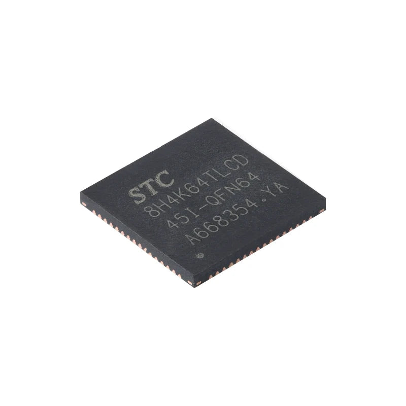
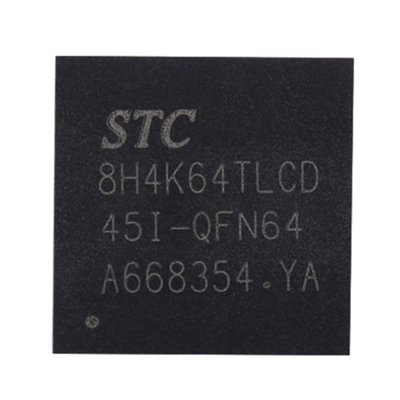
Original STC8H4K64TLCD-45I-QFN64 1T 8051 Single-Chip Microcomputer And Microcontroller MCU Chip
Original STC8H4K64TLCD-45I-QFN64 1T 8051 Single-Chip Microcomputer And Microcontroller MCU Chip
Regular price
¥2.99 CNY
Regular price
¥0.00 CNY
Sale price
¥2.99 CNY
Quantity
Couldn't load pickup availability

STC8H4K64TLCD-451-0FN64
1T 8051 single-chip microcomputer microcontroller MCU chip

Product features
Core
- The ultra-high-speed 8051 core (1T) is approximately 12 times faster than the traditional 8051
- The instruction code is fully compatible with traditional 8051
- 43 interrupt sources, with 4 levels of interrupt priority
- Supports online simulation
Working voltage
- 1.9V to 5.5V
Working temperature
- -40℃ to 85℃(The chip is manufactured at -40℃ to 125℃)
Flash memory
- MAX 64K-byte FLASH program memory (ROM), used for storing user code
- Supports user configuration of EEPROM size, 512-byte single-page erasure, and the erase and write cycles can reach over 100,000 times
- Supports updating user applications in System Programming Mode (ISP) without the need for a dedicated programmer
- It supports single-chip simulation without the need for a dedicated simulator, and there is no limit to the number of theoretical breakpoints
SRAM
- 128 bytes of internal direct access to RAM(DATA, declared using the data keyword in C language programs)
- 128 bytes of internal indirect access to RAM(IDATA, declared using the idata keyword in C language programs)
- 4096 bytes of internal extended RAM(internal XDATA, declared using the xdata keyword in C language programs)
Clock control
- Internal high-precision IRC(4MHZ to 45MHz, which can be selected or manually input during ISP programming. It can also be divided by user software to operate at a lower frequency, such as 100KHz)
- Error: ±0.3%(at normal temperature of 25℃)
- Temperature drift: -1.35% to +1.30% (full temperature range, -40℃ to 85℃)
- Temperature drift: -0.76% to +0.98% (temperature range: -20℃ to 65℃)
- Internal 32KHz low-speed IRC(with relatively large error)
- External vibration (4MHz to 45MHz) and external clock
- Users can freely choose from the above three clock sources
Reset
- Hardware reset
- When powered on and reset, the measured voltage value is 1.69V to 1.82V. (Effective when the low-voltage reset function is not enabled on the chip)
The power-on reset voltage is a voltage range composed of an upper limit voltage and a lower limit voltage. When the working voltage drops from 5V/3.3V to the lower limit threshold voltage for power-on reset, the chip is in the reset state; when the voltage rises from 0V to the upper limit threshold voltage for power-on reset, the chip is out of the reset state.
- Reset pin reset. At the factory, P5 and 4 are the default I/O ports. When the ISP downloads, the P5.4 pin can be set as the reset pin (Note: When the P5.4 pin is set as the reset pin, the reset level is low).
- Watchdog overflow reset
- Low-voltage detection reset, providing 4 levels of low-voltage detection voltages :1.9V, 2.3V, 2.8V, and 3.7V.
- Each level of low-voltage detection voltage is a voltage range composed of an upper limit voltage and a lower limit voltage. When the working voltage drops from 5V/3.3V to the lower limit threshold voltage of low-voltage detection, the low-voltage detection takes effect. When the voltage rises from 0V to the upper threshold voltage for low-voltage detection, the low-voltage detection takes effect.
- Software reset
- Write the reset trigger register in software mode
Interrupted
- Provide 4 levels of interrupt priority
- Interrupts that can be awakened in clock stop mode :INTO(P3.2), INTI(P3.3), INT2(P3.6), INT3(P3.7), INT4(P3.0), TO(P3.4), TI(P3.5), T2(P1.2), T3(P0,4), T4(P0.6),RXD(P) 3.0 / P3.6 / PI. 6 / P4.3), RXD2 (P1.0 / P4.6), RXD3 (P0, 0 / P5.0), RXD4 (P0.2 / P5.2), I squared C - SDA (P1.4 / P2.4 / P3.3), SPI - SS (P5.4 / P2.2 / P3.5) and comparator Interrupts, low-voltage detection interrupts, power-off wake-up timer wake-up, and I/O interrupts for all ports.
Digital peripheral
- There are 5 16-bit timers: Timer 0, Timer 1, Timer 2, Timer 3, and Timer 4. Among them, Mode 3 of timer 0 has NMI (Unmasked Interrupt) function, and mode 0 of Timer 0 and Timer 1 is 16-bit automatic reload mode
- 4 high-speed serial ports: serial port 1, serial port 2, serial port 3, serial port 4. The baud rate clock source FASTEST can be FOSC/4
- The 8-channel / 2-group advanced PWM can realize control signals with dead zones and support external anomaly detection functions. Additionally, it supports 8-bit timer external interrupts, 8-channel external capture measurement pulse width and other functions
- SPI: Supports master mode and slave mode as well as automatic switching between master and slave
- I ²C: Supports both host mode and slave mode
- MDU16: Hardware 16-bit multiplier and divider (supporting operations such as 32-bit divided by 16-bit, 16-bit divided by 16-bit, 16-bit multiplied by 16-bit, data shift, and data normalization)
- RTC: Supports year, month, day, hour, minute, second, and sub-second (1/128 second), and supports clock interrupt and a set of alarms
- I/O port interrupts: All I/O ports support interrupts. Each group of I/O interrupts has an independent interrupt entry address. All I/O interrupts can support four interrupt modes: high-level interrupt, low-level interrupt, rising edge interrupt, and falling edge interrupt. It provides 4 levels of interrupt priority and supports power-off wake-up function.
- DMA: Supports MORY To Memory, SPI, UARTITX/UARTIRX, UART2TX/UART2RX, UART3TXUART3RX, UART4TX/UART4RX, ADC(automatically calculates the average of multiple ADC results), and LCM
- LCD liquid crystal driver :MAX supports 4COM*40SEG; Supports 8-level gray-scale adjustment
Analog peripheral
- Ultra-high-speed ADC, supporting 12-bit high-precision 15-channel (channel 0 to channel 14) analog-to-digital conversion, with a speed FASTEST that can reach 800K(800,000 ADC conversions per second)
- Channel 15 of the ADC is used to test the internal 1.19V reference signal source (the internal reference signal source has been adjusted to 1.19V when the chip leaves the factory)
- Comparator, a group of comparators (the positive end of the comparator can select the CMP+ port and all ADC input ports, so the comparator can be used as a multi-channel comparator for time-sharing multiplexing)
- Touch keys :MOST supports 16 touch keys; Each touch key can be independently enabled: the internal reference voltage is adjustable in 4 levels; Flexible charging and discharging time Settings as well as internal working frequency Settings; Support low-power touch wake-up
- DAC: An 8-channel advanced PWM timer can be used as an 8-channel DAC
GPIO
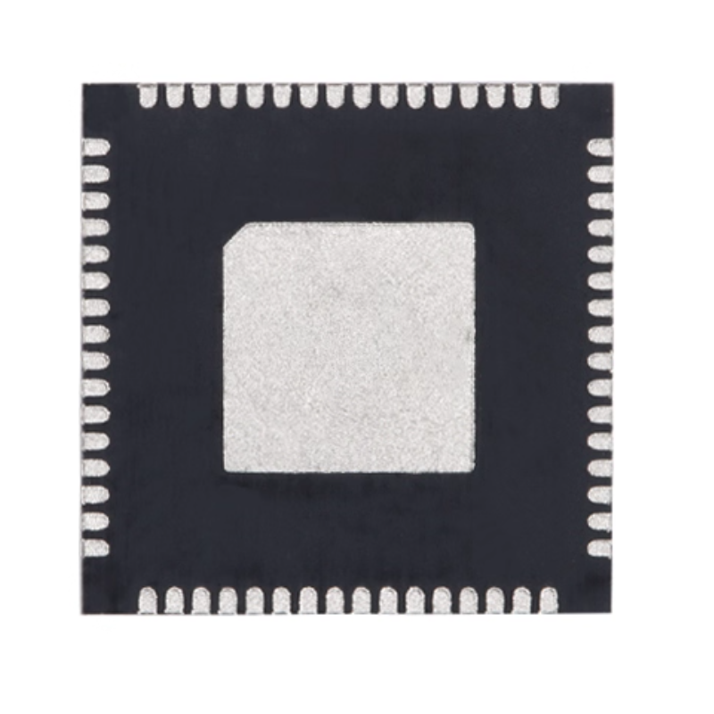
- The -MOST can reach up to 60 GPIOs :P0.0-P0.7, P10-P1.7(no P1.2), P2.0-P2.7, P3.0-P3.7, P4.0-P4.7, P5.0-P5.4, P6.0-P6.7, P7.0-P7.7
- All GPIOs support the following four modes: quasi-bidirectional port mode, strong push-pull output mode, open-drain output mode, and high-impedance input mode
- Except for P3.0 and P3.1, all other IO ports are in a high-impedance input state after power-on. Users must set the IO port mode before using the IO ports. In addition, each IO can independently enable the internal 4K pull-up resistor
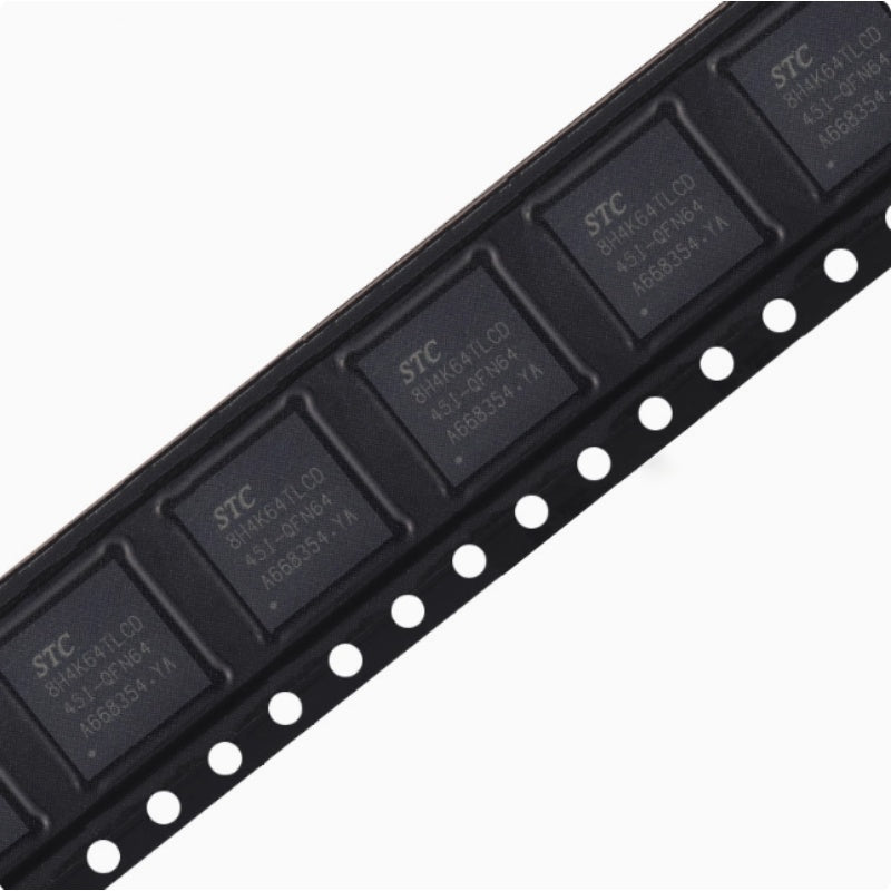
Products photography