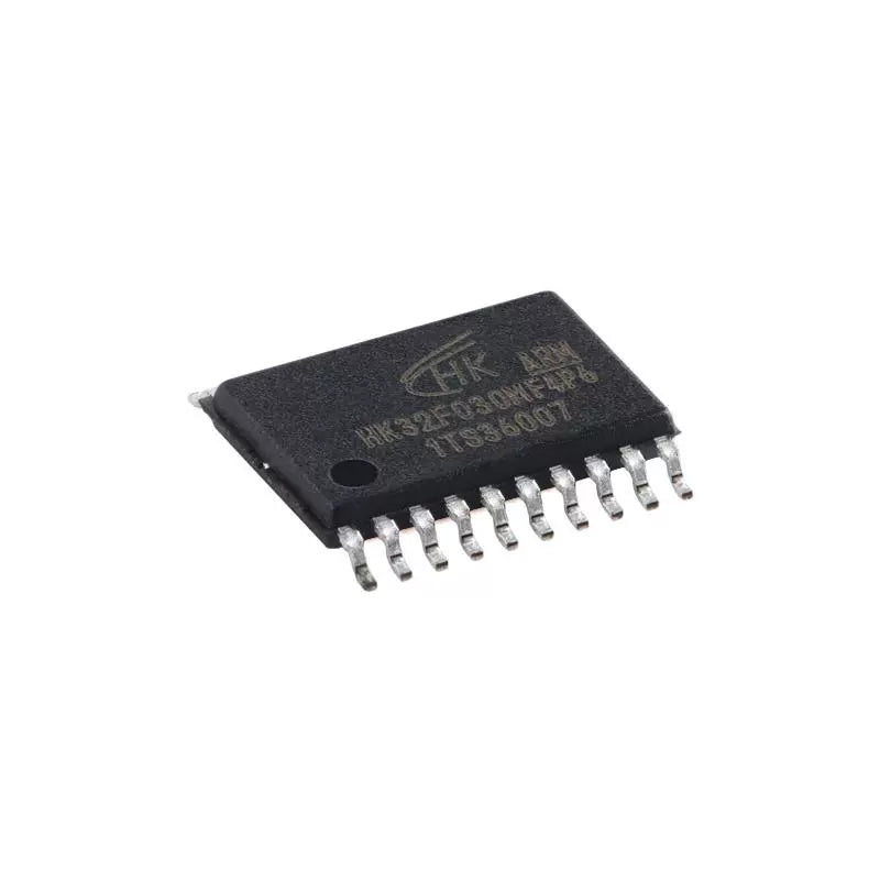
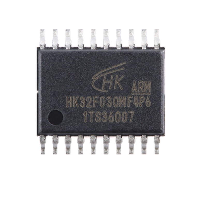
Original HK32F030MF4P6 TSSP-20 ARM Cortex-M0 32-Bit Microcontroller -MCU
Original HK32F030MF4P6 TSSP-20 ARM Cortex-M0 32-Bit Microcontroller -MCU
Regular price
¥0.53 CNY
Regular price
¥0.00 CNY
Sale price
¥0.53 CNY
Quantity
Couldn't load pickup availability

HK32F030MF4P6/TSSOP-20
ARM Cortex-M0 32-bit microcontroller -MCU

Product Introduction
The HK32F030M series uses an ARM®Cortex™-M0 core with a maximum operating frequency of 32MHz. It is equipped with 16K-byte Flash, 448-Byte EEPROM and 2-KByte SRAM. Through the register configuration of the FLASH controller, the remapping of the interrupt vector within the 16K-Byte space can be achieved.
All pins of the HK32F030M except power and ground can be used as GPIOs, peripheral IO or external interrupt inputs (the TSSOP20 package product supports 16 GPIOs): In scenarios where the number of pins is limited, the maximum number of pin signals can be provided.
The HK32F030M is equipped with multiple communication interfaces :1 high-speed (up to 6Mbps)USART, 1 high-speed (up to 18MbpS)SPI/I2S, and 1 high-speed (up to 1MHz)I2C. USART supports synchronous and asynchronous full-duplex or half-duplex communication, multi-host communication, LIN protocol, SmartCard protocol, and IrDASIR codec. The RX/TX pin positions can be interchanged by software. In the MCU Stop mode (Stop), it supports data reception wake-up. SPI/I2S supports full-duplex or half-duplex communication with data lengths ranging from 4 to 16 bits, master/slave mode, T1 mode, NSS pulse mode, automatic CRC check, and 12S protocol. The 12C supports transmission rates of 1MHz/400kHz/100kHz, master/slave mode, multi-master mode, 7110 bit addressing, and SMBuS protocol. In the MCU Stop mode (Stop), data reception wake-up is supported.
The HK32F030M is equipped with one 16-bit advanced PWM timer (with a total of 4 PWM outputs, among which 3 are complementary outputs with dead time), one 16-bit general-purpose PWM timer (with a total of 4 PWM outputs), and one 16-bit basic timer (with a scheduled output and CPU interrupt).
The HK32F030M is equipped with one 12-bit 1MSPS ADC(with an effective accuracy of 8-bit) analog circuit, one POR/PDR power-on/power-on reset circuit, and one internal reference voltage (the internal reference voltage is sampled on-chip by the ADC).
The HK32F030M supports a variety of power consumption modes. In low-power mode, the HK32F030M can be automatically awakened by the internal low-power timer.
The HK32F030M operates within a temperature range of -40°C to +85°C, with a supply voltage of 1.8V to 3.6V, and can meet the requirements of most application environmental conditions.
Product application
Programmable controllers, printers, scanners
Motor drive and speed control
Low-power sensor terminal for the Internet of Things
Unmanned aerial vehicle flight control and pan-tilt control
Toy products
Household appliances
Intelligent robot
Smartwatches, fitness bands
Product features
Operating voltage range :1.8V to 3.6V
Operating temperature range :-40°C to +85°C
Typical working current
- Run working mode :2.3mA@32MHz@3.3V(71UAMHz).
- Sleep mode :1.2mA@32MHz@3.3V(37uA/MHz), wake-up time 21nS.
- D-Sleep deep sleep mode :0.61mA@114KHz@3.3V, wake-up time 7.8uS.
- Stop stop mode :30uA@3.3V, wake-up time 10uS(can be awakened by external pin or internal timer).
CPU core
- ARM® Cortex™-M0.
- Maximum clock frequency :32MHZ.
- 24-bit System Tick timer.
- Support interrupt vector remapping (through memory configuration of the FLASH controller).
CPU tracking and debugging
- SWD debugging interface.
- ARM®CoreSight™ Debugging Components (ROM-Table, DWT, BPU).
- Custom DBGMCU debugging controller (low-power mode simulation control, debugging peripheral clock control, debugging and tracking interface allocation)Memory.
- 16K-byte Flash (128 pages, 128 bytes per page :32-bit data read, 8-bit data write).
- FLASH has a data security protection function, and read protection and write protection can be set separately.
- 448-Byte EEPROM(Byte programming time 20uS).
- 2K-Byte SRAM.
- Data Security :CRC check hardware unit.
Clock
- External high-speed clock: Supports 1 to 32MHz(1 input can be selected from 4 pins).
- On-chip high-speed HSI clock :32MHZ.
- On-chip slow LSI clock :114kHz.
Reset
- External pin reset.
- Power on and off reset (POR and PDR).
- Software reset
- The watchdog (IWDG and WWDG) timer has been reset.
GPIO port
- Supports up to 16 GPIO ports (TSSOP20 package product).
- Each GPIO can be used as an external interrupt input.
- Built-in pull-up and pull-down resistors that can be switched on and off.
- Supports Open-Drain output.
- The output drive capability is available in two Settings: high and low.
IOMUX pin function multi-mapping controller
- For small-sized packaged products (such as SO8N/SOP8), IOMUX can be used to achieve mapping control of a single pin corresponding to multiple GPIOs or peripheral IO.
Data communication interface
- 1 high-speed (up to 4MbpS)USART(supports data reception wake-up in MCU Stop mode).
- 1 high-speed (up to 1 MHZ)I2C(supports data reception wake-up in MCU Stop mode (Stop)).
- 1 high-speed (up to 16Mbps)SPI(supporting I2S protocol).
Timer and PWM generator
- One 16-bit advanced PWM timer (with a total of 4 PWM outputs, among which 3 are complementary outputs with dead time).
- One 16-bit general-purpose PWM timer (with a total of 4 PWM outputs).
- One 16-bit basic timer (supporting CPU interrupts).
- An automatic wake-up timer (AWU) operating in the Stop (Stop) mode of one MCU.
Beeper buzzer
- One Beeper buzzer can output pulses at frequencies of 1, 2, 4, and 8kHz.
- In the MCU Stop (Stop) mode, Beeper can continue to work and trigger ADC sampling at regular intervals.
Products photography