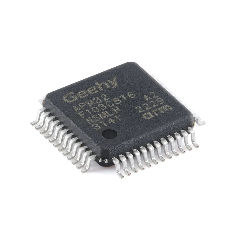
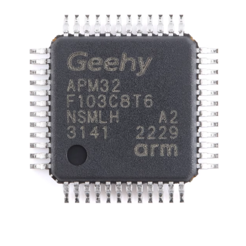
Original Genuine APM32F103C8T6 LQFP-48 ARM Cortex-M3 32-Bit Microcontroller MCU
Original Genuine APM32F103C8T6 LQFP-48 ARM Cortex-M3 32-Bit Microcontroller MCU
Regular price
¥3.70 CNY
Regular price
¥0.00 CNY
Sale price
¥3.70 CNY
Quantity
Couldn't load pickup availability

APM32F103C8T6/LQFP-48
ARM Cortex-M3 32-bit Microcontroller -MCU

Product features
System and Architecture
- ARM ® Cortex®-M3 core
- The maximum main frequency is 96MHz, and it can reach 1.5 DMIPS/MHz when accessed during the 0-wait cycle of the memory
Power supply, clock and reset
- The power supply voltage is 2.0V to 3.6V
- 4 MHz to 16MHz external crystal oscillator
- A 32KHz RTC oscillator with calibration function
- It contains an 8MHz RC oscillator that has been factory-calibrated
- 40KHz RC oscillator
- Power-on/power-off reset (POR/PDR), Programmable Voltage monitor (PVD)
Memory
- Max 128 Kbytes flash memory
- Max 20 Kbytes SRAM memory
Low-power mode
- It supports three low-power modes: sleep, stop and standby
- It supports battery power supply and can support the operation of RTC and standby registers
FPU
- Independent FPU module, supporting floating-point operations
- Two ADCs and one temperature sensor
- 1 μs conversion time (up to 16 input channels)
- Conversion range : 0 to VDDA , conversion accuracy : 12 bits
- Dual sampling and hold function
- On-chip temperature sensor
I/O
- You can choose 80/51/37/26 I/ OS, depending on the model and package
- All I/O can be mapped to 16 external interrupt controllers
- Almost all I/O supports 5V logic level input
DMA
- 7 DMA channels, supporting access to USART, Timer, I²C,SPI, and ADC peripherals
Timer and PWM
- 3 16-bit general-purpose timers, each with 4 independent channels for input capture, output comparison, and PWM
With pulse counting
- 1 16-bit advanced timer with dead zone control and emergency braking
- Two watchdog timers, including stand-alone and windowed types
- 1 24-bit self-decrement system time timer
Communication interface
- 3 USART interfaces (supporting IS07816 interface, LIN, IrDA interface and modulation and demodulation control)
- 2 I²C interfaces (supporting SMBus/PMBus)
- 2 SPI interfaces (18Mbps)
- 1 OSPI interface, supporting single-wire and four-wire access to flash
- 1 USB 2.0FS device interface
- 1 CAN2.0B interface, supporting both USB and CAN to work independently simultaneously
CRC unit
- 1 CRC calculation unit, supporting 96-bit unalterable unique identity identifiers
Debugging mode
- Serial debugging interfaces SWD and JTAG
Product Description
APM32F103x4x6x8xB/APM32E103xB series chip is based on ARM ® architecture ®- M3 kernel 32 bit microprocessor, Max working frequency 96 MHz. The built-in AHB high-performance bus, combined with high-speed memory and DMA, enables rapid data processing and storage. It is equipped with an advanced APB peripheral bus, which expands a rich range of peripherals and enhanced I/O, ensuring rapid connection and flexible control. The chip is equipped with a powerful FPU floating-point operation processing unit inside, supporting single-precision data processing instructions and data types.
Equipped with up to 128K bytes of flash memory and 20K bytes of SRAM memory, all models include 2 12-bit ADCs, 3 general-purpose 16-bit timers, 1 advanced control timer and 1 temperature sensor. It also includes standard and advanced communication interfaces : 2 I²C interfaces, 2 SPI interfaces, 1 QSPI interface, 3 USART interfaces, 1 USB2.0FS interface and 1 CAN2.0B interface. USB and CAN CAN work independently simultaneously.
The working voltage is 2.0V to 3.6V, and there are two types of operating temperature ranges to choose from: -40°C to +85°C and -40°C to +105 °C. LQFP100 / LQFP64 LQFP48 / QFN36 four different forms of packaging, different packaging of peripherals and I/O configuration is different.
Product application
Medical equipment
PC peripherals
Industrial control
Intelligent instrument
Household appliances
Absolute max rating value
If the absolute max rated value given in the max rated voltage characteristic and the max rated current characteristic is applied to the device, it may cause permanent damage to the device. Here, only the maximum load that can be endured is provided, and it does not mean that the functional operation of the device is normal under this condition. Long-term operation of the device under max conditions will affect its reliability.
Rated voltage characteristic
| Symbol | Description | Min | Max | Unit |
|
VDD- VSS |
External main supply voltage (including V and V) | -0.3 | 4.0 | V |
|
VIN |
The input voltage at the 5V tolerance pin |
VSS-0.3 |
5.5 | |
| The input voltage on other pins |
VSS-0.3 |
VDD+0.3 |
||
|
|ΔVDDX| |
The voltage difference between different power supply pins | 50 | mV | |
|
|Vssx-Vss | |
The voltage difference between different grounding pins | 50 |
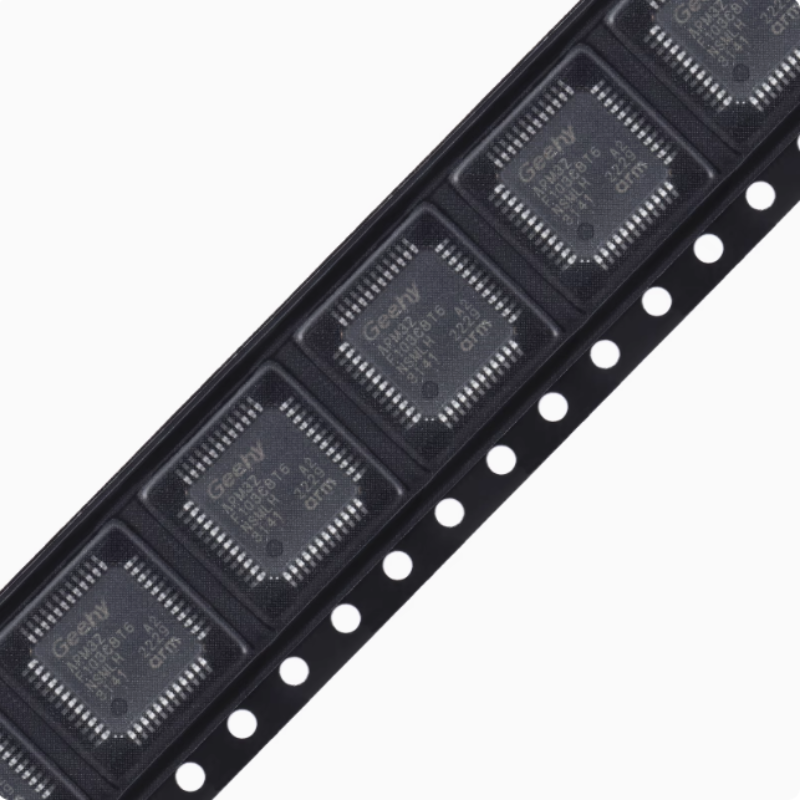
Products photography