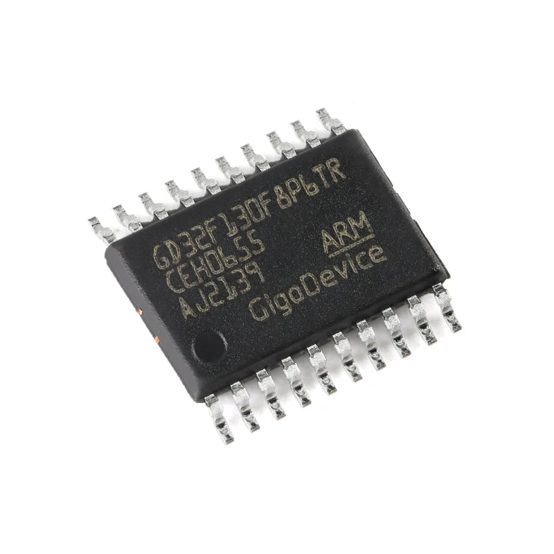
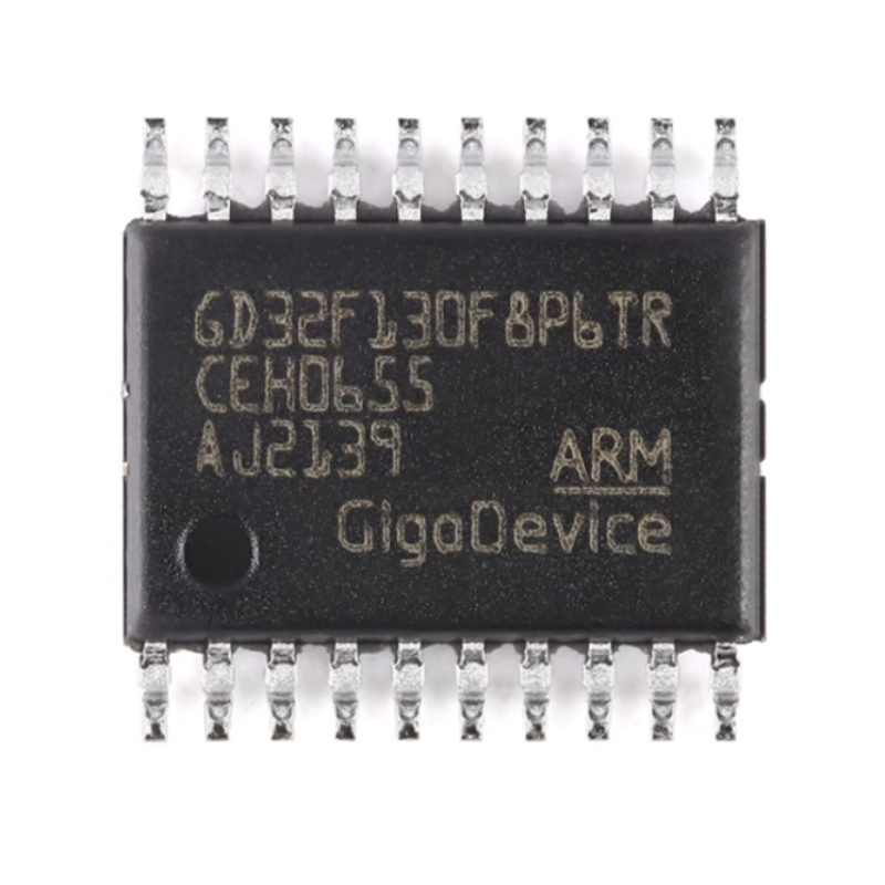
Original GD32F130F8P6TR TSSOP-20 ARM Cortex-M3 32-Bit Microcontroller -MCU
Original GD32F130F8P6TR TSSOP-20 ARM Cortex-M3 32-Bit Microcontroller -MCU
Regular price
¥3.45 CNY
Regular price
¥0.00 CNY
Sale price
¥3.45 CNY
Quantity
Couldn't load pickup availability

GD32F130F8P6TR/TSSOP-20
ARM Cortex-M3 32-bit microcontroller -MCU chip

Product Description
The GD32F130xx device belongs to the connectivity line of GD32 MCU Family. It is a 32-bit general-purpose microcontroller based on the ARM® Cortex™-M3 RISC core with best ratio in terms of processing power, reduced power consumption and peripheral set. The Cortex®-M3 is a next generation processor core which is tightly coupled with a Nested Vectored interrupt Controller (NVIC), SysTick timer and advanced debug support.
The GD32F130xx device incorporates the ARM® Cortex®-M3 32-bit processor core operating at 108 MHz frequency with Flash accesses zero wait states to obtain maximum efficiency. It provides up to 6 KB on-chip Flash memory and 8 KB SRAM memory. An extensive range of enhanced I/Os and peripherals connected to two APB buses. The devices offer one 12-bit ADC, up to five general 16-bit timers, a general 32-bit timer, a PWM advanced-control timer, as well as standard and advanced communication interfaces: up to two SPIs, two I²Cs, two USARTs.
The device operates from a 2.6 to 3.6 V power supply and available in -40 to +85°c temperature range. Several powers saving modes provide the flexibility for maximum optimization between wakeup latency and power consumption, an especially important consideration in low power applications.
The above features make the GD32F130xx devices suitable for a wide range of applications, especially in areas such as industrial control, motor drives, user interface, power monitor and alarm systems, consumer and handheld equipment, gaming and GPS, E-bike and so on.
Electrical characteristics
The maximum ratings are the limits to which the device can be subjected without permanently damaging the device. Note that the device is not guaranteed to operate properly at the maximum ratings. Exposure to the absolute maximum rating conditions for extended periods may affect device reliability.
Absolute maximum ratings
| Symbol | Paramoter | Min | Max | Unit |
| VDD |
Extemal voltage Range |
VSS - 0.3 | VSS + 3.6 | V |
| VDDA | External analog supply voltage | VSSA - 0.3 | VSSA + 3.6 | V |
| VBAT | External battery supply voltage | VSS - 0.3 | VSS + 3.6 | V |
| VIN | Input voltage on 5V tolerant pin | VSS - 0.3 | VDD + 4.0 | V |
| Input voltage on other l/O | VSS - 0.3 | 4.0 | V | |
| IIO | Maximum current for GPlO pins | - | 25 | mA |
| TA | Operating temperature range | -40 | +85 | ℃ |
| TSTG | Storage temperature range | -55 | +150 | ℃ |
| TJ | Maximum junction temperature | - | 125 | ℃ |
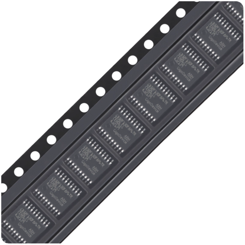
Products photography